The project describes the advantages and challenges encountered during the design of wideband continuous-time pipeline (CTP) analog-to-digital converters (ADCs). It introduces an area- and power-efficient foreground technique that exploits thermal noise to estimate the taps of digital reconstruction filters within the pipeline. The design also features a half-rate mode that leverages the CTP’s sharp filtering characteristic to reduce the back-end sampling rate, thereby lowering power dissipation. These techniques are applied to a CTP design that realises the equivalent of a 106-MHz bandwidth sixth-order Butterworth filter followed by a 12.5-bit 800-MS/s ADC. The CTP, realised in 65-nm CMOS, achieves an ENOB of approximately 12 bits in a 100-MHz bandwidth and dissipates 59 mW from a 1.2-V supply.
Motivation: This work is motivated by the inherent difficulties of designing wideband medium-resolution Analog-to-Digital (A/D) converters using traditional methods. Specifically, continuous-time delta-sigma modulators (CTΔΣMs), also referred to as CT16Ms in the source, face challenges due to the large oversampling ratio (OSR) required for sufficient noise shaping, leading to impractically high clock speeds and power consumption. An alternative, using an active filter to drive a “Nyquist-rate” ADC, also presents issues such as the need for a power-hungry drive buffer and separate optimisation challenges for the filter and ADC.
The continuous-time pipeline (CTP) ADC is presented as a compelling alternative because it combines the filter and ADC into one block, resulting in a signal chain that is significantly more power- and area-efficient, with considerably improved linearity, compared to a stand-alone filter followed by an ADC. The CTP provides inherent anti-aliasing similar to a CT16M but achieves about 2x the signal bandwidth compared to prior-art modulators in 65-nm CMOS. It also offers superior linearity and power efficiency compared to prior-art active filters.
Key Features and Design Choices:
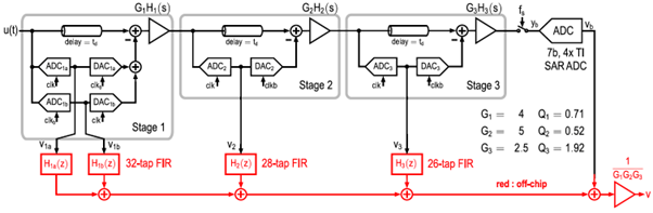
- Integrated Filter and ADC Functionality: The CTP integrates the anti-aliasing filter and ADC, offering advantages in noise, linearity, and power consumption by processing residue signals.
- Sixth-Order Butterworth Filter Equivalent: The CTP is designed to implement the equivalent of a 106-MHz bandwidth sixth-order Butterworth filter, providing a sharp roll-off beyond the signal bandwidth. This is achieved by using non-identical stages chosen to minimise STF droop across the signal band.
- No Amplifier Settling Requirement: The amplifiers within the CTP do not need to settle, contributing to power savings.
- On-Chip Digital Reconstruction Filter Estimation: A novel, power- and area-efficient foreground calibration technique is introduced, which exploits the thermal noise inherent in the CTP to accurately determine the taps of the digital reconstruction filters on-chip. This avoids the need for external calibration signals or complex off-chip computations.
- Half-Rate Mode (Implicit Decimation): The CTP incorporates a half-rate mode that capitalises on its sharp filtering STF to reduce the back-end sampling rate by half. This reduces the power dissipation of the back-end ADC and the digital reconstruction filter by a factor of two.
Performance Summary:
- ENOB (Effective Number of Bits): Approximately 12 bits in a 100-MHz bandwidth.
- SNDR (Signal-to-Noise and Distortion Ratio): Peak SNDR of 73.5 dB for a 20-MHz input, degrading to 71.5 dB at 70 MHz.
- Bandwidth: Equivalent to a 106-MHz 3-dB bandwidth Butterworth filter.
- Power Consumption: 59 mW from a 1.2-V supply in full-rate mode (800 MS/s), reducing to 52 mW in half-rate mode.
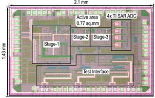
- Technology Node: Fabricated in a 65-nm GP CMOS process.
- Active Area: 0.77 mm².
- Alias Rejection: Measured raw rejection of about 48 dB in the first alias band (700–900 MHz). This can be improved by adding an upfront filter, for instance, a single pole at 200-MHz improves rejection by about 18 dB.
Contributors: Shanthi Pavan, Saravana Manivannan, Nishanth Basavaraj
References:
- Shanthi Pavan, Saravana Manivannan, and Nishanth Basavaraj, “Analysis and Design of Wideband Filtering ADCs Using Continuous-Time Pipelining,” IEEE Journal of Solid-State Circuits (JSSC), vol. 58, no. 12, pp. 3206–3218, Dec. 2023. DOI: 10.1109/JSSC.2023.3276633.
- S. Manivannan and S. Pavan, “A 65-nm CMOS continuous-time pipeline ADC achieving 70-dB SNDR in 100-MHz bandwidth,” IEEE Solid-State Circuits Lett., vol. 4, pp. 92–95, 2021.
- S. Pavan and H. Shibata, “Continuous-time pipelined analog-to-digital converters: A mini-tutorial,” IEEE Trans. Circuits Syst. II, Exp. Briefs, vol. 68, no. 3, pp. 810–815, Mar. 2021.
- S. K. Manivannan and S. Pavan, “Improved multistage continuous-time pipelined analog-to-digital converters and the implicit decimation property,” IEEE Trans. Circuits Syst. I, Reg. Papers, vol. 69, no. 8, pp. 3102–3113, Aug. 2022.
- N. Basavaraj, S. Manivannan, and S. Pavan, “Simplified simulation and measurement of the signal transfer function of a continuous-time pipelined analog-to-digital converter,” IEEE Trans. Circuits Syst. II, Exp. Briefs, vol. 69, no. 10, pp. 3993–3997, Oct. 2022.
Keywords: Aliasing, continuous, filter, pipeline, successive approximation register (SAR), time interleaving.