Logic Vertical
Overview and Significance
CMOS logic technology is a fabrication technology for creating logic devices like processors for cell phones and data centers by using complementary pairs of both P-type and N-type Metal-Oxide-Semiconductor Field-Effect Transistors (MOSFETs). FinFETs (Fin Field-Effect Transistors) have been the mainstream transistor architecture powering current processors for the last 15 years. However, attention has shifted to next-generation technologies such as Gate-All-Around (GAA) transistors, which offer superior electrostatic control, better scaling capabilities, and lower power leakage. This transition to next-gen logic technologies matters, as it directly impacts the development of High-Performance Computing (HPC) and AI infrastructure—both vital for future technological leadership.
The next stage of semiconductor advancement hinges on our ability to stretch the limits of both device materials and architecture. To achieve scaled GAA technology, work is underway in cutting-edge processes, specifically incorporating nanosheets/nanowires, refining high-k metal gate stacks, and optimizing channel materials (like SiGe).Additionally, expertise in developing next-wave devices such as Complementary FETs, forksheet structures, and 2D-material channels—technologies beyond GAA—is essential to meet growing computational demands.India is beginning to address these challenges through its India Semiconductor Mission (ISM) and other policies, focusing investment on advanced technologies and talent development.
Technical Committee members
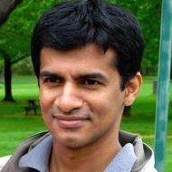
Dr. Deleep Nair
Technical Committee Chair IIT Madras |
Dr. Deleep worked for about six and a half years at the IBM Semiconductor Research and Development Center in Hopewell Junction, NY, where he served as Senior Engineer working on advanced CMOS process nodes (65nm, 32nm, 28nm and early 14nm). He also served as the lead device engineer for the multi-company 32 nm/28 nm bulk CMOS development program. His current research interests include the Design, Fabrication, and Characterization of Semiconductor Devices, RF MEMS switches and resonators, and Silicon Photonics.
|
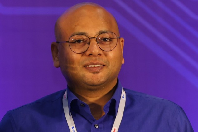
Dr. Tarun Kumar Agarwal
Academic Expert IIT Gandhinagar |
Dr. Tarun's research interests include 2D materials for beyond-silicon CMOS, emerging memory devices, and the modeling and simulation of advanced nanoscale devices. He also explores process-material-device-circuit co-design for alternative computing paradigms. He did his doctoral research at IMEC, Belgium and postdoctoral research at ETH Zurich.
|
Dr. Kaushik Nayak
Academic Expert IIT Hyderabad |
Dr. Kaushik is currently an associate professor at Dept. of Electrical Engineering, IIT Hyderabad. His research spans semiconductor device physics, mesoscopic electronics, and electro-thermal effects in nanoscale transistors, with recent work on diamond-based devices, complementary 2D-FET applications, and next-generation silicon-based transistors.
|
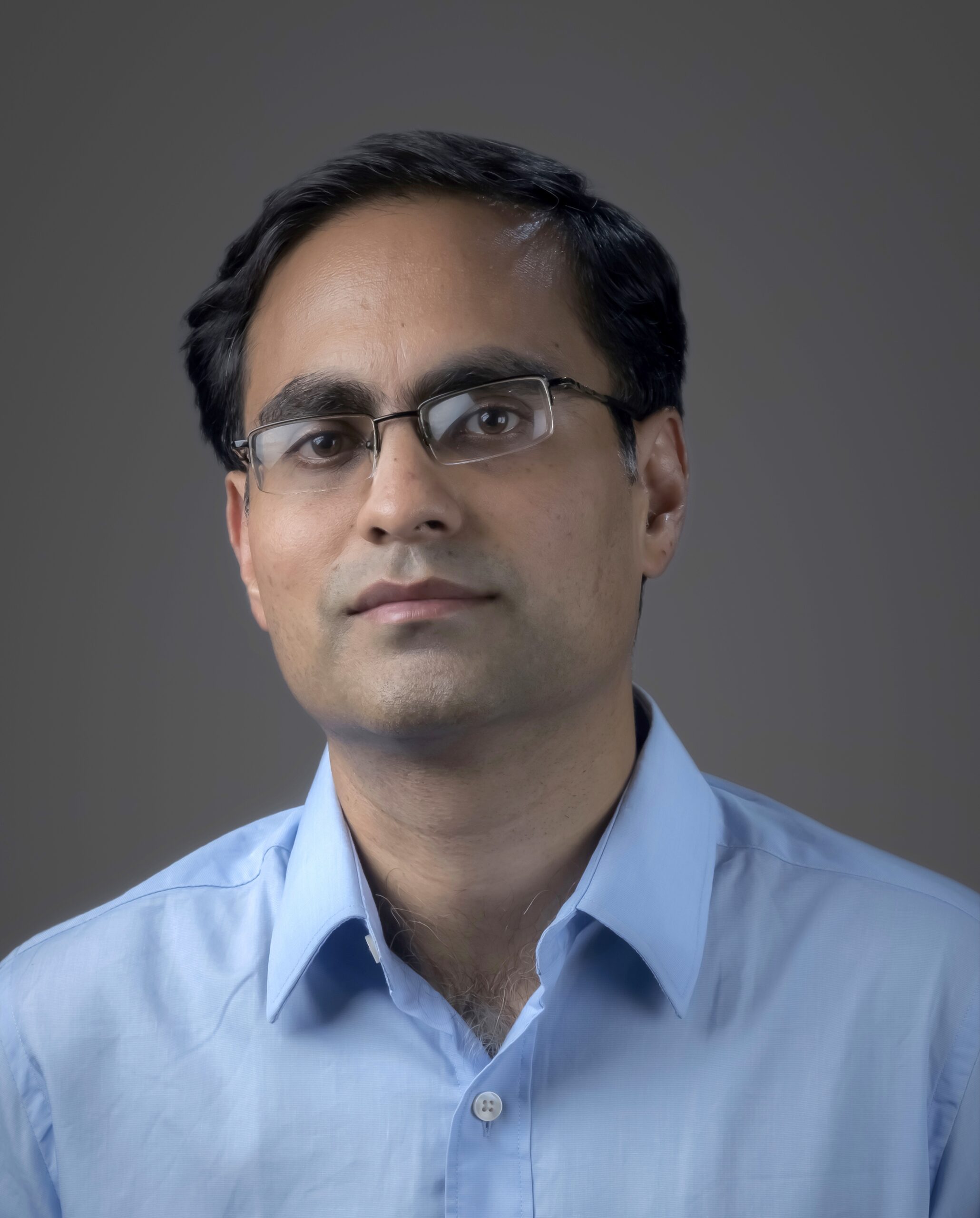
Dr. Saurabh Lodha
Academic Expert IIT Bombay |
Dr. Saurabh Lodha is the P. K. Kelkar Chair Professor at Indian Institute of Technology Bombay. Previously, he worked at Intel Corporation on the development of 15 nm and 22 nm high-performance logic technologies. Currently, his research spans wide-band-gap power devices, 2D materials, oxide semiconductors, and advanced CMOS, with end-to-end capability in design, fabrication, characterization, and simulation to deliver real-world impact.
|
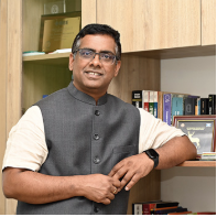
Dr. Nihar Ranjan Mohapatra
Academic Expert IIT Gandhinagar |
Dr. Nihar has worked in semiconductor industries like IHP Microelectronics, Advanced Micro Devices (AMD), and Globalfoundries for eight years. During this time he worked on different CMOS technologies and was responsible for integrating memory devices in bulk CMOS technologies. His current research interests span advanced semiconductor devices, computational lithography, Device/Compact modeling and Mixed-Signal (AMS) Circuit Design.
|
Dr. Anupam Dutta
Industry Expert Globalfoundries |
Mr. Anupam’s expertise spans MOSFET, HBT, and memory-device design, and he holds 20+ U.S. patents covering these areas. He has also worked on developing compact models for RF-SOI and bulk MOSFETs, and enabling new devices in industry-standard PDKs. Before joining GlobalFoundries, he spent nearly four years as a Research Engineer at the IBM Semiconductor Research and Development Center focusing on compact MOSFET modeling for RF-analog applications. Earlier in his career, he worked at the Indian Space Research Organisation (ISRO) and served as a Research Consultant at Indian Institute of Technology Kharagpur, where he led an analog ASIC design team for aerospace applications.
|
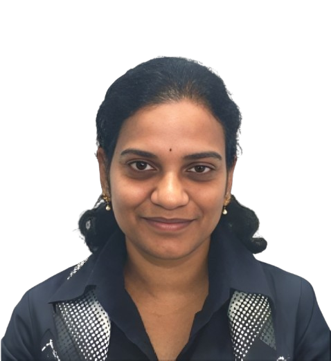
Dr. Usha Gogineni
Industry Expert Technology Development, Micron, India |
Dr. Usha is an expert in semiconductor-device engineering and chip technology for high-speed and wireless applications. She has spent nearly 13 years in leadership roles as Director of Compact Modeling at both ams AG and Maxim Integrated. Earlier in her career, she spent a decade as a Device Design Engineer at IBM Microelectronics working on silicon-germanium (SiGe) technologies.
|
