The centre of Excellence in MEMS & Microfluidics (CEMM) at Rajalakshmi Engineering College (REC), Chennai, Tamilnadu developed and demonstrated the metal embossing on glass substrate for making microstructures for microfluidic applications.
In general, glass is a preferable material by biologists and chemists due to its high transparency, inertness and easy to clean. The microstructures on glass substrates for lab-on-chip (LOC) applications are usually made by wet etching or dry etching. Wet etching using HF leads to isotropic profile, requires concentrated HF and increases the roughness whereas dry etching requires a huge investment on deep reactive ion etching facility. The team at REC is successful in making microstructures on glass substrates using a low cost technology and without the need to work with toxic chemicals.
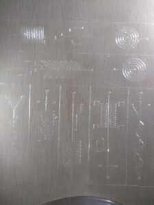
The fabrication technique demonstrated is a much simpler approach of embossing on glass using thermo-compression process with a patterned metal layer to define device structure. Well established printed circuit board fabrication photo-process is used to realize the desired planar geometry on metal layer deposited over a glass substrate. The depth of the channel is defined by the thickness of the metal deposited by electro-plating. The embossing technology offers a relatively safer approach conducive to batch processing to enable repeatable, high-yield low-cost devices fabricated using low-cost equipment. A thermo-compression system has been custom fabricated for this purpose. Key features of this system are programmable and precise control over temperature profile as well as press head movement with the active press in a vacuum chamber. Major challenges of achieving adhesion of deposited thick nickel layer without peel-off and control of the thermo-compression process to achieve reliable and repeatable embossing without structural distortions. Research and development work in this activity has been focused on addressing and resolving major issues discussed above and optimal process steps for low-cost microfluidic device manufacturing have been well established. The cover glass is another borosilicate glass wafer with inlet and outlet ports formed in alignment with the microfluidic structure at the bottom. This cover glass is bonded successfully with the bottom glass substrate by thermal bonding (also called as direct bonding) using the same thermo-compression system at the same softening temperature used for embossing with a load of around 200 kg. This metal embossing on glass substrate is also proved for manufacturability with a full wafer. This technology is ideal for LOC applications with microfluidic structures for deep channels, microfluidic channels integrated with nickel heater structures for localized heating, microfluidic channels integrated with microelectrodes for electro-chemical sensing etc on glass substrates.
Reference:
- P. Madhankumar, L. Sujatha, R. Sundar and Gautham Viswanadam, “Fabrication of Low-cost MEMS Microfluidic devices using Metal Embossing technique on Glass for Lab-On-Chip Applications”, J.Micromech. Microeng. 33 (2023) 084001 (1- 14) https://doi.org/10.1088/1361-6439/acd8c3; IF:2.3
Technology Transfer: Technology is transferred to Semsil Technologies Pvt Ltd, Bangalore
Funding Agency: Department of Science and Technology, Government of India.
Compendium: https://drive.google.com/file/d/1wAWHHgXoP6jiRfu38-X7_hK3FzWfcvK9/view?usp=drivesdk
Keywords:
Microfluidics
Embossing
Adhesion
Thermo-compression
Photo-process